Apple TV Box Teardown

My teardown object is the 3rd Generation Apple TV Box, which was first released in the market in 2012.

Exterior Outlook

The box is 4 inch by 1 inch tall. The back side of the box features an AC Adapter port, HDMI output port, Micro-USB (for service and support), optical audio out port, and a 10/100 base ethernet port.

Material Breakdown
Material weight/breakdown
The Breakdown

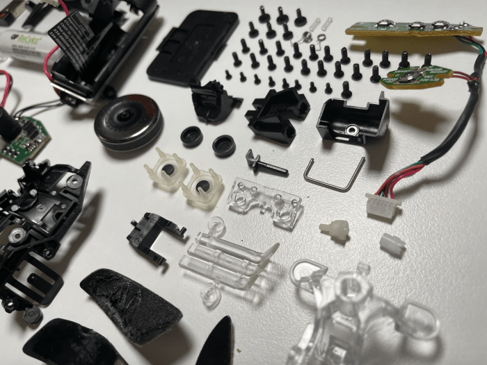
Step 1: The first challenge was to remove the core of the rubber-coated base from the upper case. Using an X-acto knife, I was able to loosen the parts from one another and using a metal spludger, I snapped it open and the base popped right off.

Step 2: Once open, the base is secured with a metal heat sink. To remove the metal sink, I used a screwdriver to release the 5 screws.

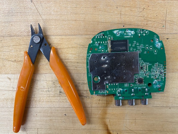
Step 3: The logic board is held in place by the power supply connector (recycled plastic) and using a metal spludger and pliers, I was able to disconnect it and free the logic board. The power supply rating is 3.4V at 1.75 A.

Step 4: Using pliers, the status LED is freed from the metal pad.

The logic board has a few elements that required some research and understanding.

  • The single core processor is the application processor with Apple A5
  • Toshiba THGVX1G6D2HLA018GB NAND Flash- is an interface which handles essential functions, including writing block management, error correction and driver software. It simplifies system development, allowing manufacturers to minimize development costs and speed up time to market for new and upgraded products.
  • Broadcomm BCM4330 – single chip device which provides the highest level of integration for a handheld wireless system
  • SMSC LAN9730 standalone USB to ethernet controller – Microchip’s LAN9730 was specifically designed to provide a high-performance, low-cost USB to 10/100 Ethernet connectivity solution with a Hi-Speed Inter-Chip (HSIC) interface.
Remote Control Teardown

Material: Aluminum casing

Tools and techniques: X-actor to remove the different buttons and feedback chips.

Features: Bluetooth wireless technology, IR transmitter and Lightning connector for charging

Observations
  • All the components are housed on the logic board, which means that if it breaks, it could be expensive to replace.
  • This product is ultra-compact
  • PVC free
  • Made with recycling materials (100 % recycled aluminum in the Remote, 100% recycled tin in the solder of the main logic board and 35% of recycled plastic in multiple components)

Oregon Scientific Weather Station Teardown

Model: BAR 806; Solar, Wireless

The Oregon Scientific BAR 806 is a wireless, solar weather station. Its LED display showcases forecasted weather, time and date of day, and temperature. Also, despite the “solar” attribute, it is not fully solar — the solar capabilities are an environmentally friendly way to save energy and prolong battery life. Lastly, the device did not turn on so I decided to start the teardown (especially since it’s capabilities are overshadowed by an iPhone’s weather app).

Tools

  1. Heat gun: for any glue/adhesives.
  2. Multitool (mainly pliers): to pry, pull and hold pieces.
  3. Pencil: to press on small pieces during the teardown and knolling process.
  4. Xacto knife: to make small cuts to snap off, open up and pry pieces.
  5. Screwdriver: unscrewing screws.

Steps

These show how I got inside the weather station. I pried the buttons off, along with the glass for the led screen, which separated the front from the back.

Once the back was open, the PCB was exposed and I began to remove each piece either by hand, screwdriver or plier to get ready for knolling.

Here are some process shots removing wires, circuit boards ontop of circuit boards, radio transmission springs, etc.

Lastly, I took a heat gun to the LED screen (in an attempt to remove the film) but no success, so I began to knoll the pieces.

Components, Materials, Parts

Parts of the Weather Station (Knolled image on the left)

Components of the Circuit Board (layered PCB with copper paths — I actually learned from Anne that they are double-sided and you are not viewing the back of one side on the other).

  1. Resistors: “R”, reduce the flow of current, are seen along each other in a series and are within yellow boxes on the circuit board.
  2. Capacitors: “C”, store electrical energy and are primarily seen on the large circuit board as Red, Green and Black “Chiclet” shapes.
  3. Diodes: “D”, allow current to flow in one direction, and look like a small fire extinguisher.
  4. Transformers: “T”, transfer power from one device on the circuit to another, and look like a match on the left side of the large circuit board .
  5. Integrated circuits: “U”, are microchips with many functions, such as storing memory, and are within black boxes or circles on this circuit board.
  6. Antennas: “antenna” or “H”, they transmit and receive signals. One on this circuit board is located on the upper right side and is a white box with a “3”. It is the humidity sensor.
  7. Transistors: “Q”, they amplify or control electrical signals, and are micro-sized black boxes on this circuit board.
  8. Black “Blobs” are components/chips encapsulated by epoxy. For this circuit, some control the LCD (on the larger PCB) while some process information from the sensors (on the medium sized PCB) to determine Barometric pressure.
  9. “EU/UK” Switch in the middle to toggle between radio signals.
  10. EM94AB (on the medium sized circuit): semiconductor for data regarding the Barometric pressure and weather clock.
  11. Unmarked semiconductor (on the small circuit): most likely for data of the temperature sensor.

Design Takeaways

This Weather Station is definitely unique and it’s interesting to see how all of the technology is packaged (I assume by machine) within the object encasing itself (for both indoor/outdoor use), and also on the circuit boards. It is so much data, energy and storage within such a small piece of hardware — very cool. Also, since many chips on the board have black epoxy over them, I have concluded that most of the technology is proprietary to the company as they also cannot be found on the internet. Then, it is interesting to see the various methods to achieve the same result, as seen from the antennas and transmitters for transmissions/signals. Lastly, I appreciated the switches for a user to toggle between Celsius and Fahrenheit (for weather) and EU/UK (for radio signals).

Google Home Mini Teardown

I changed my object from Netgear wi-fi extender to Google Home Mini, an old generation model I do not use anymore. It is the smallest and the cheapest model in Google Home family. I was always wondering about how big and clear sound it makes considering its size (and price range).

Fast forwarding the teardown

As you can see in the video, it consists of four main parts – Top shell (with Primary PCB attached to it), aluminum frame, Speaker driver and bottom shell.

What fascinated me during the teardown was acoustics engineering of this little gadget. If you look into it, you can easily see why Google Home Mini has wonderful sound for its size. First, speaker driver is almost as big as Home Mini itself. Second, aluminum frame which is between the top shell and the speaker driver functions as a sound diffuser which spreads sound horizontally throughout the room.

(1) Top shell
– Plastic frame covered with fabric
– Primary PCB (including dual microphone and 4 LED indicator)

(2) Aluminum frame
– Plastic pieces (Black) for better Antenna performance (Wi-fi)
– Omni sound diffuser

How sound travels inside Google Home Mini

(3) Speaker drive

(4) Bottom shell – it has power input (micro USB) and toggle switch for microphone on/off.

Magic Mouse 2 Teardown

For this project I did a complete teardown of Apple’s Magic Mouse 2. This product, originally released in October of 2015, offered a new integrated lithium ion internal battery making it rechargeable. If you ask me, the rechargeable aspect of it is kind of dumb, due to the fact that the charging port is in the bottom, making it useless while it is charging. Six years have passed since this product came out and apple has yet to change this, so they are definitely up to something.

The teardown of the mouse was quite difficult because it was mainly glue holding the object together. It gave me the impression that they don’t want the average consumer looking into how they manufacture their products. So I started picking the plastic rails from the bottom with a box cutter in order to cut away the glue until I had enough surface to pull the whole piece out. After that I started prying open the top part with my fingers and realized that it was held by these four plastic clips that were part of the main tray that held the battery, as well as the motherboard and most of the electronics. Once I exposed the motherboard, I took apart all of the screws with a tiny screwdriver, this just mainly took apart the spring that would make the mouse click.

By the end of the teardown, the only thing I had left to do was to take out the battery. This was probably the most tricky and scary part due to the fact that it was completely glued to the plastic tray. I was kind of skeptical about taking it apart because I once poked a lithium battery and it did not go well. so I carefully went about it and managed to take it out using a flat screwdriver to pry it out of the case.

Motherboard Parts:

  • ST Microelectronics STM32F103VB 72 MHz 32-bit RISC ARM Cortex-M3
  • Broadcom BCM20733 Enhanced Data Rate Bluetooth 3.0 Single-Chip Solution
  • Unknown 303S0499—probably a proprietary Apple touch controller
  • NXP 1608A1 Charging IC
  • Texas Instruments 56AYZ21

Mouse Parts:

  1. Bottom sliding rails
  2. Motherboard
  3. Click Switch
  4. On/Off Switch
  5. Lithium Ion Battery with Lighting Port
  6. Top Cover and Touch Sensor Array
  7. Aluminum Base
  8. Plastic Tray

Waterproof Bluetooth Speaker

Materials used: Waterproof plastic with a matte soft touch finish, silicone rubber button casing, Lithium Polymer battery, iron or Aluminum speaker (which includes a cylinder plate, magnet, basket with a soft wire mesh cloth for the “spider” and “cone”, and a dust cap at the end, see diagram below for a speaker breakdown!).

Looking up the parts and chip numbers on the circuit board was no easy task. I managed to find a couple but not all. (see list below)

A1SHB: P-Channel Trench Power MOSFET (The A1SHB uses advanced trench technology to provide excellent RDS(ON), low gate charge and operation with gate voltages as low as -2.5V. This device is suitable for use as a battery protection or in other switching application.)

SS14: Surface Mount Battery Rectifier (Guarding protection, low forward voltage, reverse energy tested, high current capability.)

K8002D: Electronic Component Integrated Circuit (ICs) which functions as an amplifier — in practice denotes any semiconductor-based chip comprising an integrated set of digital circuitry

2TY: Silicon Epitaxial Planar Transistor

J3y: Plastic-Encapsulate Transistors (Complimentary to S8550)


I used a pair of clippers, a magnifying glass and my bare hands to tear this speaker open. There wasn’t much to it really, just some brute force.

I do love the overall circle motif of the speaker’s design. Every outer surface piece of this was rounded, from the button interface to the plastic suction cup at the back. I thought this was a lovely extension of the circularity of the internal shaping of the speaker mechanism.

I also do appreciate how compact this speaker was built – the LiPo battery was stuck onto the circuit board with 3M double sided tape, with no indication of the battery voltage or care for alignment. The somewhat haphazardness of the construction of this item subtly implied the story behind who put this together and how potentially speed was valued over precision.

Roku 1 Media Streamer + Remote Teardown

Roku 1, Remote, and Charger before taken apart

List of the tools and techniques you used to take it apart

– Small screwdrivers for wedging the plastic casing apart and unscrewing the PCB from the bottom casing.

Multiple screwdrivers were needed since it was so tightly shut

– Large flathead screwdriver for prying the casing open.

The yellow screwdriver provided enough support and force to yank it open.

– Small wire-cutting plier for cutting the faraday shields.

The shield came off very easily with this plier

Materials and techniques used for each component

Overview of all the parts

1. Roku’s and Remote casing – made out of ABS plastic. The plastic is heated and injected into a mold to take the shape of the case.

2. Faraday shield – made out of thin aluminum. Made to enclose and block electromagnetic fields.

3. Toshiba TC58NVG1S3HTA00 flash memory – made out of plastic/epoxy

4. Button pad – made out of silicone rubber using a mold. The design and color are UV printed.

5. Circuit board – made out of a combination of prepreg, laminate, copper foil, soldermask, nomenclature, final finish.

Chips

1. Toshiba TC58NVG1S3HTA00 – storing data?

2. Samsung K4B4G1646D-BYK0 DRAM Chip – storing data?

3. Broadcom BCM7218 – The brain of the system

4. Broadcom BCM43143 – Wifi IC.

Two interesting design elements

1. The Roku’s plastic case is very tightly shut. I assumed that it was held together with glue since it was so difficult to pry apart but ended up finding no glue at all. It was designed with edges that lock the parts together which does a good job securing all the parts within so that no one will unintentionally open it. 

2. The sheet of buttons is also very fascinating. The way all the raised buttons are connected on a sheet to make sure they all stay together and in order so nothing will get lost or reorganized. 

Serato Scratch Live (Teardown)

…breaking down an audio interface

Teardown Timelapse

Parts & Materials

Step 1. Step 2. Step. 3

Step 4. Step 5. Step. 6

This extremely rugged, portable, high quality, bus-powered USB interface features 2 switchable phono or line inputs, a microphone input, 2 line outputs, and pass thru outputs for the phono/line and mic.

  • USB Input: bring power to the unit
  • RCA: For audio input and output connectivity 
  • Audio Gain Knob: adjust volume of pass thru

– Motherboard

  • Isolated ac/dc converter : An isolated power converter isolates the input from the output by electrically and physically separating the circuit into two sections preventing direct current flow between input and output, typically achieved by using a transformer.
  • Programmable Logic Device: provides speed and power customization. Critical portions of design can run at high speed while remaining portions run at reduced speeds.
  • High speed/ high temp 4 channel digital isolator: data transfer and signal isolation

Tools & Techniques

Screw Driver – used for removing screws connecting the side panels to the top and bottom pieces of the interface

Small Slip Joint Pliers – used in unscrewing the potentiometer nuts fastening the 1/4” jack inputs to the front and rear panels

Design Takeaways

One initial aspect of this design that I noticed right away, was that the input and output connections were inlaid, creating an overhang from the top and bottom slabs of metal. The top and bottom extend exactly the same length outward as the RCA connections. I believe this was deliberately done to prevent damaging the RCA and 1/4″ connections during use or travel. Without this design decision they would stick out making them much more susceptible to breaking off.

Another aspect of this design which I believe to be deliberate, is the shape. The short and wide design provides for a very stable object, limited the chances that is will fall or move while in use. This shape also gives the object a very low profile increasing its ability to fit in to smaller spaces or allow other tools to sit on top of it.

iPod Video Teardown

2006 iPod Video 30GB | Model: A1136

This was actually my iPod from 2006! It was in my pocket everyday till I got my first iPhone in 2012. After that, it lived in the center console of my car for occasional tunes and then in my desk drawer as an Ebenezer of simpler times.

It was still functioning in all ways till this assignment. The hard drive whirred quietly, the LCD screen had no spider cracks or bleeding, and the hold switch (though filled with dirt and grime) still switched.

Though I appreciate the clear polycarbonate coating that covers the black faceplate and becomes the window to the screen, it’s fillet of the back cover continuing through the headphones port that is my favorite detail. In older models of the iPod, the opening of the headphones port is completely perpendicular, but A1136 incorporated this detail to allow the curve of the mirror polished back cover to remain uninterrupted.

The assembly of A1136 is exceedingly simple. It’s held together more by double sided tape and plastic clips than it is by screws. However, without specialty tools, this proved difficult to disassemble. I resorted to deforming the tip of a metal pallete knife to separate the back cover and face plate enough to expose the plastic clips. From there, I gently folded it open and removed the 12 screws that secured the different components to the aluminum frame and back cover and removed all double sided tapes and padding.

Treadmill Monitor Teardown

Pre-Teardown

The victim of my teardown is a treadmill monitor. It has push buttons and an LCD panel on the front side. On the backside, it has a metal piece to hook onto a treadmill and a lidded slot for two AA batteries.

The Teardown

The outer carcass of the monitor is held together by a small handful of screws that are easily visible on the backside. Though rusty, these were easy to remove.

On the inside, a large circuit board with myriad parts is firmly attached to the bottom of the carcass with small screws. These took effort to remove. The push buttons however, popped right off.

It was surprising that the screen was taped onto the carcass with mere tape! You could definitely tell how old this item was from that yellowed color….

A- Always B-be K-Knolling (if you don’t get it see this)

The Parts

The circuit boardtechnically a Printed circuit board (PCB), is made of a series non-conductive material layers (like fiberglass) that conceal copper circuits that run along the board. Most copper circuits are protected by a thin green laminate (which can easily be scratched off!) that superficially illustrates where the copper wires lie. Some copper circuits however, are revealed, like in the case of the push-buttons and the LCD screen. Here is a cool PCB breakdown by layers graphic that I found.

The six golden squares and rectangle on the right hand side are areas of revealed copper circuitry.

PCB boards are manufactured in factories by a series of cutting machines, drilling robots, edge-polishing machines, plating the with boards copper, printing the circuit diagrams on the boards, and so on and so forth. This video shows the complete process.

LDC screen – is made of liquid crystal material, which I don’t really know what it means, but it looks like it is made of a series of glass and other very thin sheets of polarized film and films with electrodes.

The encasing – the rigid plastic enclosure that protects and keeps in place all the electronic parts of the monitor, as well as the buttons and batteries. Likely injection-molded in a factory.

The buttons – made out of hard plastic and rubber, the buttons are injection molded, then the inscriptions on them are (probably) UV printed by machines.

Back To the Board

On the monitor’s PCB board are the following:

  • One TC4069UB Hex Inverter, which is responsible of inverting the signal received (if IN is LOW, then OUT is HIGH; of if IN is TRUE then OUT is FALSE)
  • One LM324N operational amplifier which responds to a small input signal and produces a larger output with the same characteristics as the input.
  • Plenty of resistors (R) of different line colors. Resistors are used to reduce current flow.
  • Several 104 round ceramic capacitors (C), as well as larger cylindrical capacitors. Capacitors store electrical energy.
  • Diodes (D). Diodes act as one-way-switches for current, meaning that it enables a current to flow in one direction, but prevents it to flow in the other.
  • Connector Jacks (J). Connector jacks are used to connect sub-sections of a circuit together.
  • Transistors (Q). Which look like short cylinders out of which a slice has been taken off. Transistors are responsible for regulating current, of for amplifying a signal into an even greater signal.
  • Switches (S) (apparently, though they don’t look like it). Switches are responsible
  • Meters (M). Meters measure the currents and voltages in a circuit without changing them.

Other terminology that I looked up:

  • Blowers/motors (B)
  • Terminals (E)

List of Tools and Techniques for Teardown

-Large screw driver star bit to detach the monitor mount from the monitor

-Medium screw driver star bit to open the monitor encasing

-Small screw driver star bit to internally dismount the circuit board from the monitor’s encasing.

-Snippets to cut the wires joining the circuit to the speaker.

My Favorite Design Elements

  1. The revealed copper circuitry int he areas where the buttons and LCD screen are touching the circuit board. It is elegant and I like the bit of reveal.
  2. The push-buttons, starting with the fact that the markings on them are still intact. This means the designers really considered the fact that users would be sweating, and selected the most lasting printing method.

Questions for Becky:

On the board, there are some components that look like one thing, but the markings label them as another thing. For example, I see what looks like a transistors that is marked as E B C on the board. I’m confused about why that is.

Logitech Mouse Teardown

Tools I used: 

  • 8-in-1 Precision Slotted and Philips Screwdriver
  • A single driver
  • 4 double-sided bits include #000, #00, #0 and #1 Philips tips and 1/16 in., 5/64 in., 3/32 in. and 1/8 in. slotted tips

It’s my first time fully tearing down a mouse and the result surprised me. I have not imagined before how many components/parts can go into one fist-sized mouse after laying them all out on a flat table. For example, just the internal body part consists of 22 screws, which is more than some furniture that I have built. During my teardown process, I also realized how some parts are specifically made to be more adhesive and difficult to dissemable.

For example, I was stuck at the very first step, trying to figure out how to get into the inner parts of the mouse. Then I found out that the screws were all hidden under the nylon feet with adhesive materials under the mouse. I am impressed at how the mouse included the nylon feet to cover the screws to make the design as a whole look seamless while providing a smooth surface to support the mouse to better sense the movement.

Some other difficulties I came across was taking apart the scroll wheel that was fixed with a spring and a few plastic pieces that helps stabilizing it while scrolling. Taking apart the scroll required the help of a second person. Also, the metallic piece located on the left side of the mouse that lets the finger rest was tightly attached to the main surface with adhesive, so I tried using a screwdriver to pry it open with force, but I ended up breaking it into two pieces.

After unscrewing all the tiny screws located below the exterior body parts from the mouse, there are many little round “buttons” that lock the three main body parts together. I inserted the screwdriver into the slit between the body parts, and tried lifting it from one side first and as the gap in between gets bigger, I break apart the body parts like how I would open a crab.

The first part of the mouse that I like is the OMRON D2FC-F-7N switch which serves as the mouse’s right and left clicks. How it functions is that there’s a leaf spring under the microswitch that reflexes when we hit on them and it only works when the leaf spring is placed at the very bottom notch of the microswitch. A click will send electrical signals via metallic contact to the computer. This is the core of a mouse and always wanted to know how it responds when interactions occur. 

The second component of the mouse that I found interesting was the Atmega324PA microcontroller. This is the microchip that enables the mouse to run. It is incredible to see how a finger-sized chip can store so much data and information to make a mouse functional. For example, this microchip alone has “32 KB ISP Flash memory with read-while-write capabilities, 1 KB EEPROM, 2 KB SRAM, 32 general purpose I/O lines, 32 general purpose working registers, a real-time counter, three flexible timer/counters with compare modes and PWM and many more.” And this microchip operates in a single clock cycle that delivers specific instructions throughout to balance the power consumption and the processing speed. 

Logitech Performance MX Mouse Parts:

  • 4 nylon feet
  • 1 scroll wheel with a black locking pin
  • 2 springs for the scroll wheel
  • 2 Double-click culprit: OMRON D2FC-F-7N switch
  • 22 mouse internal screws
  • 8 small Philips head screws
  • 4 screws that hold the two body parts
  • 4 PH1 and 2 T5 screws on the bottom
  • 3 exterior body parts
  • 1 interior body part
  • 1 internal plastic clip under thumb rest
  • 1 flat flex ribbon cable/connector
  • 1 Atmega324PA microcontroller (enables the mouse to run)
  • 1 circuit board
  • Nordic NRF24L01 chip with trace antenna (Bluetooth wireless communication) 
  • 1 power switch
  • 1 battery holder 
  • 1 battery cap
  • 1 thermistor within the battery housing to prevent over-temperature
  • 1 optical mouse lens
  • 1 USB dongle
  • 1 optical encoder