Jabra Pro 9400 Duo / Mono Teardown – Yukti Arora

The Product : Jarba Pro 9400 Duo/ Mono

The Product

For my teardown, I got the Jabra Pro 900 Duo/ Mono, a wireless headset that enables employees to take calls from their mobile, desk and softphone all with one headset. 

It uses DECT technology to provide wireless talking, just like landline cordless devices, allowing users to move away from  150 meters/450 feet away from their desk without dropping the call. These headphones are designed for call centers or office purposes. So  great about this headphone is that it can work with multiple phones. 

The Teardown : 

The Teardown.

1. The headset stand, which has a monochrome screen, had covered screws and after finding the right screw driver, the Torx T6, I opened back to reveal a circuit board. 

The headset stand revealed a circuit board.

2. Then I moved on to the headphones,  for which I tore apart the two cushioned sides. Which further revealed three more screws, which were Torx T3 screws. 

3. On  the non headphone side, I saw that it had a magnet behind. I further learnt that magnet here help with the speakers. 

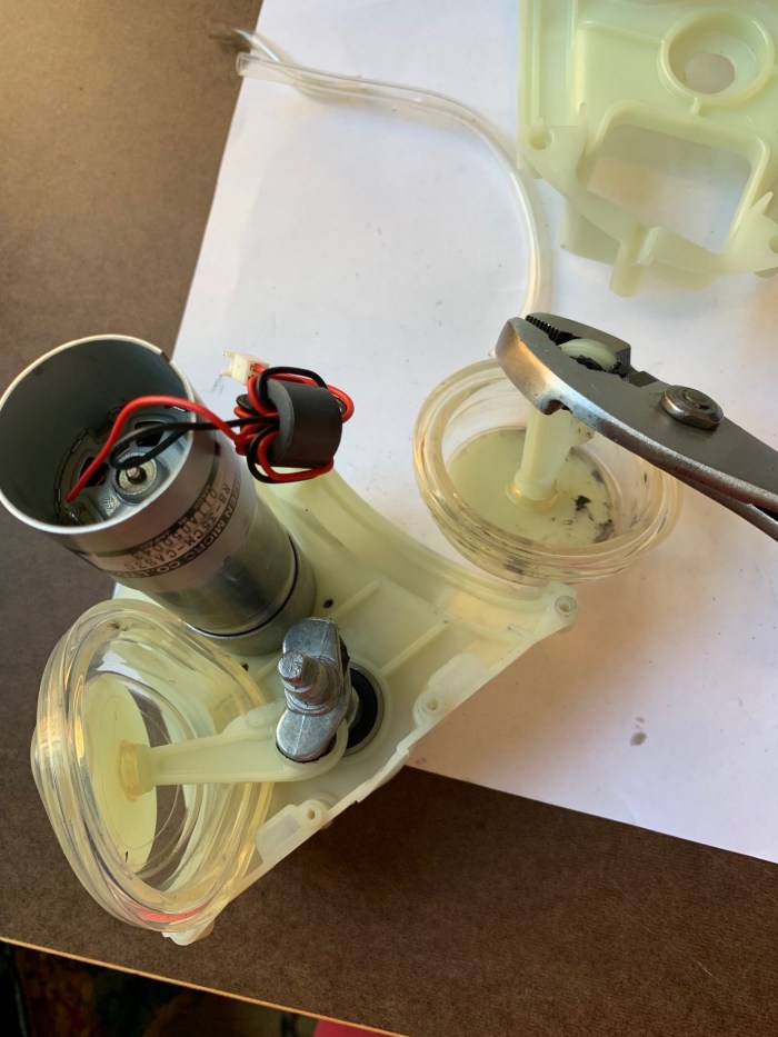
4. On the other side of the headphone where, we also had a speaker mic, the headset also had lithium batteries, copper wires and a part that helped with the rotational adjustment of the speaking area. I learnt that the copper wire is voice coil. It acts as an electromagnet for whenever the current passes. 

The copper wire, which acts as an electromagnet for the headphone speakers.

Tools used to open the part. 

1. Torx T6 & T3

2. Flathead 1mm

Materials that were used in this headset : 

1. PVC , through injection moulding machines.  

2. Rubber

3. Artificial Leather

4. Memory Foam

5. Copper wires

6. Circuit Board

7. Metal Charging plates

8. Wires

9. Screws

10. Silicone screw covers

11. Sealing wax etc.

What I loved about these headphones is that the headphones stand, also serves as a charging device which makes it easy for the user to worry about, running out of battery, unlike even some very expensive models, where you have to charge the headset separately. This device felt very similar to the cordless phones and the way they  charge and the designers here probably took the inspiration from there. 

Thanks for reading. Hope you got to know a little more about wireless headsets used in settings where the job is to be on the phone all the time. 

Spectrum TV Remote Teardown

The Teardown

Initially, when starting to disassemble this TV Remote, I was stumped. I did not see any screws to take this apart. After asking my classmates, I took my exacto knife and started to try to unfasten the outside shell of the remote. After getting a few clasp unfastened, the remote fell apart pretty easily. All the pieces inside were big and easy to disassemble. I was overall really pleased with how easy this process was for me!

Tools Used To Take it Apart

  • Exacto Knife

Parts Breakdown

Materials Used + Manufacturing Techniques

While searching for information on the parts and materials used in this remote, I came across this article that summarizes the processes and parts used in different types of remote control. I will be quoting information from the article in this blog post!

A. Circuit Board

From what the parts tell me, this remote has a PCB or a printed circuit board.

A PCB is “an electronic circuit with lines and pads that connects various points together allowing signals and power to be routed between physical devices. It is made by combining different sheets of non-conductive material, such as fiberglass or plastic coated with a very thin layer of Copper on the Top side that easily holds electronic circuit. 

The PCB process starts with heating and cutting of CCL sheets, chemical pre-treatment and brushing, CCL sheets are then sent for masking, etching and drying. After whole manufacturing process PCBs are sent for Bear board testing and Visual QC check. Then these PCBs are sent for mounting.

Mounting is done by two ways:-

  • Through Hole Technology (THT)
  • Surface Mount Technology (SMT)

Once mounting is done these PCBs are again tested and are sent for further proceedings. These all steps integrate and provide error free PCBs.”

“Electronic components are assembled on printed circuit boards. The components which are assembled on most remotes are integrated circuit also known as an IC… In this circuit, the IC works when a key is pressed. It then translates the key into a sequence code, with a different sequence for each different key. The IC then sends these signals out through the IR/RF to its receiving end or dedicated device for which remote is made for.”

Remote Control Contact Spring

“Remote Battery Contact Springs are manufactured on precision CNC forming machines by using high quality material such as steel and stainless steel wire.”

B. Outer Shell AKA Plastic Cabinets

The plastic cabinet of this remote was most likely polycarbonate plastic or acrylic but there are many options depending on the product requirements, “such as acrylic, polycarbonate plastic, ABS, nylon, silicone, styrene and thermoplastic polyurethane, known as TPU and thermoplastic elastomers, or TPEs.”

Injection moulding is a likely technique used to mold the pieces and printing, screening, or designing is used in post-processing.

C. Keypad

The keypad is made out silicone rubber and

This PDF showcases all the buttons’ functions on the keypad.

D. Plastic Layer with Holes for Buttons

I think this piece’s use is to provide structure for when the button is pressed to come into correct contact with the corresponding spot on the circuit board.

It seems to be made out of plastic, and the technique was most likely through a mold!

Design Elements

A. Small cylinder to hold parts in place

What I like about this element is it is a very simple solution to what could be a huge consideration when design a small device with many parts. This small column allows for easy assembly and disassembly but also provides a dumb and easy way to keep all the elements in their correct position.

B. Backlight button

The second element I like is the button with the sun on it. It provides the user with the ability to backlight all the buttons in case their environment is too dark to see in. I think the placement is easily accessible and the icon is easy to understand. Mostly, its function solves for a particular pain point while many users watch tv in the dark.

iPhone 5 Teardown

The iPhone 5 is a smartphone that was designed and marketed by Apple Inc. It is the 6th generation iPhone, succeeding both the iPhone 4 and iPhone 4S. It was formally unveiled as part of a press event on September 12, 2012, and subsequently released on September 21, 2012. The iPhone 5 was the first iPhone to be announced in September, and setting a trend for subsequent iPhone releases, the first iPhone to be completely developed under the guidance of Tim Cook and the last iPhone to be overseen by Steve Jobs.

Here’s my teardown time lapse: https://www.youtube.com/watch?v=kzUFn1ksF-4

The iPhone 5 featured major design changes in comparison to its predecessor. These included an aluminum-based body which was thinner and lighter than previous models, a taller screen with a nearly 16:9 aspect ratio, the Apple A6 system-on-chipLTE support, and Lightning, a new compact dock connector which replaced the 30-pin design used by previous iPhone models. This was the second Apple phone to include its new Sony-made 8 MP camera, which was first introduced on the iPhone 4S.

The iPhone 5 has the joint second-shortest lifespan of any iPhone ever produced with only twelve months in production.

Parts List:

There are a TON of components on this phone..

Here’s an example of how many are on the logic board alone:

  • Qualcomm PM8018 RF power management IC
  • Hynix H2JTDG2MBR 128 Gb (16 GB) NAND flash
  • Apple 338S1131 dialog power management IC*
  • Apple 338S1117 Cirrus Logic Class D Amplifiers. The die inside is a Cirrus Logic device (second image) but it does not look like the audio codec.
  • STMicroelectronics L3G4200D (AGD5/2235/G8SBI ) low-power three-axis gyroscope—same as seen in the iPhone 4S, iPad 2, and other leading smart phones
  • Murata 339S0171 (based on Broadcom BCM4334) Wi-Fi module
  • Skyworks 77352-15 GSM/GPRS/EDGE power amplifier module
  • SWUA 147 228 RF antenna switch module
  • TriQuint 666083-1229 WCDMA / HSUPA power amplifier / duplexer module for the UMTS band
  • Avago AFEM-7813 dual-band LTE B1/B3 PA+FBAR duplexer module
  • Skyworks 77491-158 CDMA power amplifier module
  • Avago A5613 ACPM-5613 LTE band 13 power amplifier

Materials & Processes:

The back of iPhone 5 is made of anodized 6000 series aluminum which was machined to its dimensions using a CNC mill. Then the Aluminum is textured and polished. Finally finished of with a diamond blade cut on the chamfers for a mirror-like finish.

After this process, an image is taken of the housing and is matched to the closest fitting piece out 725 cuts.

The computer chips are made up of silicon, and plastic, and the metal wires used to create the layers of circuits are made of copper or aluminum. Silicon is obtained from either silica sand or from quartz.

The lens cover is made of sapphire. This is because sapphire is thinner and more durable than the cover glass on your iPhone 4/4S and because keeping optics in pristine condition is crucial for camera performance.

Finally, my thoughts:

The iPhone 5, in terms of form, is the best looking and feeling iPhone of all time. The chamfered edges and finish feel amazing in hand. When they switched to curved edges on the iPhone 6and broke away from the squared off edges and chamfers us in the iPhone 5, I dropped my phone waaay more. I think Apple really hit the nail on the head with the manufacturing processes for surface finish, fit, and materials.

PUGZ Leaking [wireless earphones] – Teardown

SVA MFA PoD
Making Studio
Assignment 1 – Teardown of an appliance/electronic device.

“Charge while you listen to Music”

PUGZ is tiled the World’s smallest wireless earbuds (as of 2015) which can be charged through your phone or any electronic device that you are carrying!

The Designers specify PUGZ to have minimal size & shape which allows perfect fit and music experience!

PUGZ was started its production officially in 2014 and started their distribution form 2015 through 2016.

We are looking at a specific model of PUGZ for this assignment which is the PUGZ Leaking .
The PUGZ leaking is manufactured with “ear gel design” that directs the audio into your ear but lets you hear a bit of your surroundings.

OTG Charging

The power backup for PUGZ is said to be very sustainable it uses 3% of your smart phone battery capacity to charge your PUGZ you get 4.5 hours of music and 10 days of standby. You can also plug into your phone and listen while charging, often called ‘OTG’ On the go charging.

The USP behind PUGZ is in the Go charging facility. Apart from this the designers’ were solving also for these issues :

  • Generic earphones are too Big
  • Bluetooth earphones run out of batteries
  • Lightweight, minimal in size.
  • Sweat proof – IP64
  • Microphone – 6th gen dual-mic cVc® advanced audio enhancements and noise suppression

Teardown


The Integrated Bluetooth ROM is part of the Qualcomm CSR8645 series.

The CSR8645 is a dual-mode (Audio output and microphone input) ROM Chip is designed to offer extensive voice and music capabilities in a ROM-based package, including

aptX [aptX is a proven technology that compresses and then decompresses audio as it travels from a source device like a phone, to a receiving device like a wireless speaker, in a way that it can be transmitted over Bluetooth without damaging the quality. ] and

cVc [clear voice capture) noise echo cancelling and noise suppression technology is designed to transmit crystal clear voice quality when making calls.]

Making it ideal for a variety of wireless audio products with support for voice and music. The CSR8645 has a range of silicon platforms for wireless audio applications which integrate a dual-mode Bluetooth radio, an application processor, a battery charger, memory and various audio and hardware interfaces into a single-chip solution. The CSR8645 is an easy and cost-effective platform for developing …more

Typically This model is chosen for 3 reasons :

– High performance Audio
– single-chip designs
– 2-mic audio technology

OTG Functionality

The OTG – On the Go charging is made available by “open circuit” system that is completed using magnets. The switch system is built using 18k gold and is connected using gold wires to a copper wiring system.

The charge plates on the charger and the earphones are connected using a magnet.

The product in itself it made of plastic, rubber, wire, circuit boards, and gold.

The entire circuit system and speaker is enclosed in a thermoplastic casing which is is given a gloss finishing. The sound filter is made up of metal.

The wires are as most wires made up of copper. The wire system has 4 wires consist of a common ground and; left earphone +, right earphone +, and microphone.


When dismantling the product I did misinterpret a lot of the parts in terms of how the were manufactured or what the part was attached in the system. May be this will give you a an idea of how it was

Here are some honest Customer reviews

When I connected it to my phone as well I faced the below 2 issues

– The Bluetooth connectivity was very poor, and

– The earphones did not work unless connected to the charger

Why did the designers do it this Way?

2 design Elements that absolutely Boggle me are :

1. Standard Vs. Sports Earbuds – What really confused me or kept me thinking was when I used the earphones the standard earbuds kept falling off the ear, whereas the sport earbuds were intact despite jumping or running. When inspected closely the standard earbuds had a flat base which was to be inserted into the ear. We all know our ears are not hat simple. So the flat base did not hold still against the protruding ear walls and kept sliding off.

The Sports model also had the same design for the “in-ear” part – it was flat too, but what kept it in position was that there was is extra “grip-bit” on the outside. It acted like a counter force to against the ear somewhat like a lever system, which put pressure from the outside while the in-ear piece was pushing it out, a perfect push-pull scenario!

2. The “SQUIRCLE – The designers have on multiple posts and videos mentioned the unique shape they have used for designing – the Squircle – neither a square nor a circle.

if we speak in terms of design this shape just confuses me!
The shape to my eyes in not very satisfactory to look at and feels asymmetrical

in terms of conducting electricity. Square shaped conductors have sharp corners and Electric field is not uniform when we consider any shape with corners e.g. square, rectangle etc., and negative charge accumulates at corners.

In circular shape have their own advantages and disadvantages – advantages being more!- from what I have read about them, depending on may factors such as the amount or charge they are holding material type and thickness circular objects have more usability in electronics. So unsure of why Circle was not considered?

Microsoft Arc Touch Mouse Teardown-shun cheng hsieh

It was such an elegant and well built wireless mouse

At the first glance, I thought this is a PowerPoint wireless controller.

However, I notice the part made out of silicon seems floppy and has some wrinkles on it. I tried to bend it through its wrinkles, and after a “click” sound it become a shape that can support our hand. At that time, I realize this is a mouse. After removing the battery cap and the name of this product “Microsoft Arc Touch Mouse” indicates itself as a mouse.

It’s hard to find screws these days. After searching, I realize the first two screws were hidden under the sticker. Remove these two screws and you will notice there are more screws above the silicone part. After removing those, you can easily take off the silicone part.

At the silicone part you can notice parting line on the side which indicates this part is an silicone injection part. soft material injection are widely used in shoes outsole and remote control button. Soft material injection usually have more visable part line and surplus materials may need hand trimming. Therefore, it’s easier to tell their part line. The glossy parts of this mouse are also made throuht injection modling. The material may be ABS or PLA.

The arc part is pretty complex the parts are fastend by aluminum rivets. I tried to reomove all these rivets but I only cut a little piece of rivet. That’s why I assuming the materials of riverts are made of aluminum. I aslo found some nice clean explosion view of this product.

credit: Carbon Design Group

In this project I use mostly small screwdriver and sometimes diagnoal cutting plies. It was pretty surprised that screwdriver can disassameble most part of this mouse.

The interesting part of this product must be magnatic part that can hold use connector. It may not have enough sapce for designer to put controllor in battery cabinet as most wireless mouse do because this mouse is very thin.

magnetic holder

The second design part I really appreciate is the arc part. It’s comeplex and delicate and this series have arc type of structure in every generation. The 1st generation was simply a fold structure. This concept may want to save some storage space for user. I’m pretty impressed by the hard work of both designer and engineer. Can’t wait to see next generation of Arc Touch!

Arc Mouse 2012 ver.

Amazon Kindle Teardown

Assignment 1

Introduction

The Amazon Kindle is one of the most popular ebook reader in the United States. It was exciting to get this product to unravel its inner workings.

The Kindle 2 and its AC adapter.
Cracking open the back.

Closer look of the inside of a Kindle.

Tools used to take apart the Kindle 2

To remove the Back Casing(1) of the product I used a metal chisel. I must say this was an exciting look into a product with electronics. I then used a screwdriver to remove the small screws and lifted the logic board and display assembly out of its plastic housing.

Disassembled: Front View

The Back Casing (1) and Front Casing (2) are made from Plastic that is obtained from oil through the process of injection molding. The Back Casing has speaker holes on the top right and left. Amazon is not discrete about what plastic they use for the production. However, when we are done using our Kindle we can send it back to Amazon and they will properly dispose it. The Keyboard (3) seems to be a blend of plastic and rubber. It’s has an elasticity, when we press any key, it comes back to its original position. The Metal Case (4) is a part behind the Electrophoretic Display (5). The display is held by a “window frame” of adhesive on the Front Casing (2). After a couple of gentle twists I was able to separate these parts. The Electrophoretic Display (5), is made of tiny titanium dioxide, hydrocarbons, black dye and oil.

Disassembled: Back View

The Keyboard (3) fit into the Front Casing (2). 16 screws (6) attach the Front Casing (2) to the Metal Casing (4).

Disassembled: Back View

The back of the Electrophoretic Display (5) has a mirrored shinny appearance and is sandwiched between these two pieces. The lower end of the Display is attached with a copper coated piece known as a Flex Circuit Connector (11) Flex circuits are typically manufactured in China using a polyimide (Kapton) material and one to multiple layers of copper. It is responsible for allowing electrical circuits to flow through the device. The Lithium Ion Battery (7), Controller Board (8) and EMI Shield (9) are secured with screws on the grey area of the Metal Case (4). The Lithium Ion Battery (7), is a rechargeable power source that is made using heavy metal such as Lithium, Cobalt and Lead making it extremely important to dispose correctly. The battery is Model No. S11S01A. It’s a 3.7 V, 1530 mAh lithium polymer. The Controller Board (8) is used for video cards and Random-access memory (RAM) which allows connection of different video source inputs to be selected and shown on a screen. The EMI Shield (9) is a metal piece attached on top of the Controller Board (8) to prevent electromagnetic interference (EMI) or radio frequency interference (RFI) from impacting sensitive electronics. The black piece (10) is attached to the red and black wire. It looked like a plastic part that felt like the control for the exterior button

Disassembled: Back View

The Logic Board (12) contains 7 chips that are protected by different EMI Shields (13). It also has a wireless card (16) that was inserted in its own Card Casing (15).

Close-up of Logic Board

The wireless card (16) is by Oberthur Technologies , a French digital security comment that enables the Kindle to connect to the internet via radio wavelengths. Most of the chips are made by Freescale, Samsung and Epson. The main processor of the Kindle 2 is the Freescale chip which is  labeled MCIMX353DjQ5C M99V BTHV1052C SNGPR (12 A). It is a 532 MHz, ARM-11 90nm 14mm package. The MC13892AJVL CTGL 1103K (12 B) is a Freescale battery management chip that is made in china. The Samsung semiconductor K4X1G323PC -8GD8 (12 C) is a Mobile-DDR SDRAM chip. There another Samsung SDRAM chip, KLM4G1EEER (12H). The WM8960 (12 D) is a low power, high quality stereo codec designed for portable digital audio application. The Atheros Chip (12E) supports for Kindle’s WiFi.  The Texas instrument SN92009 A2 TL 11L A14G G4 (12 F) is the power management chip. The co-branded Epson and E-Ink chip (12 G) is the display controller. It is a PFBGA package that supports “high speed screen updates (2048×1536 at 50Hz+) 

All the parts

Interesting Design Elements:

The redesign of the Kindle 2 from its first generation seemed to have cleaner lines and carefully designed proportions. Despite new models, the Kindle 2 still has an evergreen design and personally I love the white. Additionally, the Kindle 2 is a good example of Design for Disassembly. I only required 2 tools (Metal Chisel and a Screwdriver) to take the whole tablet apart. This helps facilitate future changes and dismantlement for any parts that need to be replaced and recycled.

Avent Electronic Breast Pump Teardown

Carter Brigham

Original Item
1st Step
Open
Open alt angle
Remove tubes
Unhook
Exposed screws
Separate
Separate alt angle
Remove motor
Remove board
Out
Unscrewed
Diaphragms
Gears
Motor
Hand pull
Remove diaphragms
Wrenched
Gear Molds
Gears disconnect
Saw hard plastic
Sawed down
Knolled

The materials in the pump were hard plastic (high-density polyethylene- HDPE), plastic tubing (polyurethane), gears (steel, gear oil, magnet), flexible diaphragms (polyurethane, hard plastic fittings to attach – HDPE), clips (HDPE), screws (steel), screw covers (polyurethane), circuit board (copper-plated fiberglass material, epoxy resin, polyamide and polyester film), resistors (metal, PVC insulation), capacitors (electrodes, metal plates, dielectric insulating material, ceramic material), microchip (semi-conductor material, silicon, wires -copper, PVC insulation), motor (steel, wire, brush, electro-magnet, gear oil).

Manufacturing techniques needed to make a breast pump include, but are not limited to, injection molding for hard plastic (reciprocating screw, venting air, coolant, ejector pins/sprue removal, stamping), machining aluminum mold for injection mold (16,000 lb machine, reamers, end mills, torque wrench, gauges, cobalt steel twist drill, coolant), electrical wire (copper block, lubricated pulleys dye and stretch, low voltage conductors, insulated plastic extrusion machine, coat with PVC, precision laser confirm uniformity, cool in water trough, stamp information, voltage test), plastic tubing (vacuum hose, dry, augers mix, heat, extruder, heat, cool in trough, pulled through water through rollers, laser measure uniformity, pull by conveyer), gears (automated band saw slice, drill, cool, turret with blades drill, stamp, titanium cutter shape gears’ insides, gear hopper cuts outside, furnace, inject with carbon, grinder), circuit board (cut board, apply resin and film, etch, chemical bath), resistors, capacitor, motor, microchip (ventilation, vacuum to maintain dust-free space, cut silicone, oxidize in furnace, centrifuge, stepper exposure machine, plasma etching).

To take apart the breast pump I used a Phillips-head screwdriver, a wrench, hand saws and my hands.

The designers chose to create a device that allows the machine to mimic the woman’s own baby’s sucking rhythm. By manually pumping, she can press a button on the handle when she finds a match. The machine will then repeat or ‘remember’ the timing. I don’t understand how this works but it is the selling point of this model.

An electric breast pump exists because the diaphragm covers the breast and the motor pulls at regular intervals mimicking the real experience so milk is released and expressed into an easy-to-use container. The action begins with sharp, short pulls of suction and then increases to longer and stronger motions. As a working mother this invention made my intentions for the health of my babies what I wanted.

Limerick PJ’s Comfort Breast Pump Teardown

Parts of the Breast Pump

  1. Hard Plastic Case
  2. Two silicone control knobs on top
  3. Silicone Tubes with three way plastic connectors
  4. Mother Board
  5. Motor (Inside – Copper wire encased in a cylinder which is creates a magnetic effect)
  6. Five part rotor disc made of silicone and plastic and attached to the motor
  7. Copper wire wrapped with cello tape and encased in a cuboid
  8. Seven Black and Red Wires coiled together and attached to the motherboard
  9. Wide silicone strips holding the motor in place
  10. Absorbent foam inside a plastic cylinder
  11. Sixteen nails
  12. Bolts
  13. Washers

Tools used to take it apart of screw drivers

  1. Philips and Slotted Screw Drivers
  2. Xacto Knife
  3. Hands

Design elements I liked about the device

  1. The colour
  2. The curved and old telephone like shape of the object

Both of these elements make it seem a bit more approachable and familiar device.

Bop It BLAST Teardown

Xinyue

Pre-Teardown

What I teardown is bop it. It was originally a talking and glowing guy, and the way to interact with it was mainly pressing the center part, pulling the blue feet and twisting the green feet. A round head contains the most important circuit boards and springs, and its two feet are mainly where batteries, some extended wires, buttons, small circuit boards, and mechanical parts are placed.

The Teardown

I first removed the shell on one side with a screwdriver and found that the battery is on its legs, not on its head. The buttons are located above the left leg and touch a small circuit board.

When I removed all its shell, I can see that the main chip is placed on its head. On the head chip board, there are various circuits extending to its legs. The ports of the circuit are connected with battery, buttons, lights and beads.

Next, I started to disassemble its head. When the plastic fixing piece was removed, a spring jumped out. This is why the head can be pressed.

When I further disassembled its head, a speaker was pasted on the back.

At this point, it still has the other half of the head that I haven’t removed it yet. You can see that the orange button corresponds to the button on the chip.

There is still a spring inside this half of the head, and a red lamp bead behind it.

Next is the teardown of the two feet, I will use a video to illustrate.

Knolling

1. AA battery 2. Speaker 3. Fixed cover 4. Spring 5. Battery cover 6. Silicone button  7. Button  8. Shell 9. Screw(and Square nut) 10. Plastic lever 11. Polyethylene slider 12. Control button 13. Chip 14. Battery holder 15. Lamp bead 16. Circuit 17. Rebound spring

Manufacturing technique used to make it

Injection molding

Chips Sheet

  • Debounce time setting(when you press on your standard mechanical switch, it hits the contact and then it bounces briefly from momentum of you hitting the key/switch, sometimes the momentum can be enough for the contacts to touch again and cause a double click. Debounce time is basically and amount of time that the switch doesnt register another click.)
  • D1-D7 (Diode)
  • Q1-Q3 (Tertiary tube)
  • MS (Synchronous motor)
  • GS (Synchronous generator)
  • SP- (Speaker?)
  • GND (Ground)
  • BR (Bridge rectifier filter)
  • T1 (Transformer)
  • BB (Thermal relay)
  • JMP1-JMP2 (Jumper?)
  • 8OZVC116-MANRO1H
  • C1-C3 (Capacitance)
  • P20、P30、P33 (Electric power)
  • R1-R15 (Resistor)
  • J1-J2 (Jumper)
  • BG (Backside Grinding)
  • QB (Quit button?)
  • Q4 (Tertiary tube)
  • VCC (Voltage)
  • BB (Thermal relay)
  • 8OVC116-KEYBRO1H
  • D3、D4 (Diode)
  • S1 (Switch)
  • SP-、SP+ (Speaker?)
  • VC116-KEYCRO1H
  • S1 (Switch)
  • P/T (?)

Tools used

  1. Screwdriver
  2. Scissors

Design elements I am interested in

  1. Put the battery on its legs not in its head. (In addition to the realization of the function, the internal parts distribution must also consider its appearance. Its legs have just enough space for the battery, and it is easier for users to teardown.)
  2. Use the user’s pull and twist to press the button. (Make full use of the user’s behavior and use mechanical buttons to save costs.)

iPhone 6 Teardown

Tools & Technique
Pentalobe screwdriver
Sanding tool (used as an improvised plier)
Heat gun

One of the most difficult parts was just getting this iPhone open. The screwdriver was only able to remove one tiny screw at the bottom of the iPhone that holds the phone together. Luckily the screen was slightly popping from that lower half of the phone so I was able to stick a small sanding tool in the corder and twist to separate the two halves. After that it was many many tiny screws and a bit of heat to separate the battery from the base.

Serial Numbers
8212172a – Camera light sensor
H2jtfg8yd1bms – Memory
1971-a 821- LCD digitizer

The Process
Since the iphone was neatly designed to split into two halves I worked on one half at a time.

Side 1: Screen side with parts for camera, microphone, home button, earpiece

Side 2: Bottom side with parts for sim card, LCD, vibration, volume, speaker camera battery, circuit board (memory), sim card

Manufacturing

USA: The blueprint, crystal, specialized parts and processors
Japan, Korea and Taiwan: display panels, chipsets and memory
Europe: gyroscope
Mongolia: Rare earth minerals
China: The final manufacturing

The body of an iPhone is made by aluminum milling and finishing with diamond tools. It takes about 400 steps to assemble the iPhone, including polishing, soldering, drilling and fitting screws. That doesn’t include all of the more complex processes and chemical engineering for things like the battery and processing chip.

Interesting Design Features

I think one of the most interesting things about the interior of the iPhone is how neat it is. It reminds me of the UX design where everything is perfectly placed. It’s incredibly well organized and perfectly splits into two halves. I think this was intentional so that parts were easily fixable. I also think this type of design is in engrained in Apple’s ethos.

The other thing I noticed is that the memory and processing chip are encased. It is not possible to see the chip itself (as far as I know). I think the designers did this as an added layer of protection since that is the brain of the machine…After googling I found this was done to protect the chip from Electromagnetic interference.